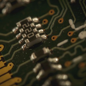
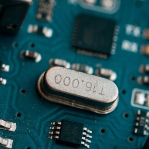
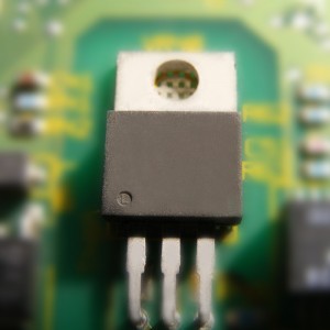
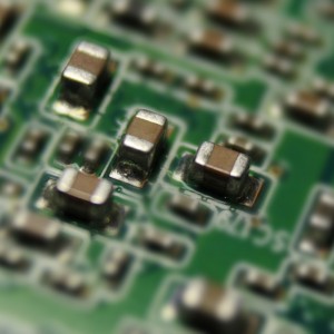
Mosfet purchase service for switching circuits

About This Item
The main advantage of a MOSFET is that it requires almost no input current to control the load current, when compared with bipolar transistors (bipolar junction transistors/BJTs). In an enhancement mode MOSFET, voltage applied to the gate terminal increases the conductivity of the device. In depletion mode transistors, voltage applied at the gate reduces the conductivity.[2]
The "metal" in the name MOSFET is sometimes a misnomer, because the gate material can be a layer of polysilicon (polycrystalline silicon). Similarly, "oxide" in the name can also be a misnomer, as different dielectric materials are used with the aim of obtaining strong channels with smaller applied voltages.
The MOSFET is by far the most common transistor in digital circuits, as billions may be included in a memory chip or microprocessor. Since MOSFETs can be made with either p-type or n-type semiconductors, complementary pairs of MOS transistors can be used to make switching circuits with very low power consumption, in the form of CMOS logic
The basic principle of this kind of transistor was first patented by Julius Edgar Lilienfeld in 1925.[1]
The structure resembling the MOS transistor was proposed by Bell scientists William Shockley, John Bardeen and Walter Houser Brattain, during their investigation that led to discovery of the transistor effect. The structure failed to show the anticipated effects, due to the problem of surface state: traps on the semiconductor surface that hold electrons immobile. In 1955 Carl Frosch and L. Derick accidentally grew a layer of silicon dioxide over the silicon wafer. Further research showed that silicon dioxide could prevent dopants from diffusing into the silicon wafer. Building on this work Mohamed M. Atalla showed that silicon dioxide is very effective in solving the problem of one important class of surface states.
Following this Atalla and Dawon Kahng demonstrated a device that had the structure of a modern MOS transistor. The principles behind the device were the same as the ones that were tried by Bardeen, Shockley and Brattain in their unsuccessful attempt to build a surface field-effect device.
The device was about 100 times slower than contemporary bipolar transistors and was initially seen as inferior. Nevertheless Kahng pointed out several advantages of the device, notably ease of fabrication and its application in integrated circuits.[3]